Fermi Level In Semiconductor / Why is the fermi level of p type semiconductor increased ... - It also lies closer to the conduction band than the valence band.
Fermi Level In Semiconductor / Why is the fermi level of p type semiconductor increased ... - It also lies closer to the conduction band than the valence band.. It is a thermodynamic quantity usually denoted by µ or e f for brevity. The fermi level pinning effect is strong in many commercially important semiconductors (si, ge, gaas), and thus can be problematic for the design of semiconductor devices. Adding even a single impurity atom to a semiconductor nanocrystal with a diameter of 4nm, which contains about 1000 atoms, leads to a nominal doping level of. In an ohmic interface, the total current density j entering the interface is a function of the difference in the equilibrium fermi levels on the. The position of the fermi level with the relation to the conduction band is a crucial factor in determining electrical properties.
In an ohmic interface, the total current density j entering the interface is a function of the difference in the equilibrium fermi levels on the. The density of electrons and holes, energy level and fermi level, the direction of movement of majority carriers, etc. The position of the fermi level with the relation to the conduction band is a crucial factor in determining electrical properties. 7 10 cm 19 3. Adding even a single impurity atom to a semiconductor nanocrystal with a diameter of 4nm, which contains about 1000 atoms, leads to a nominal doping level of.
Elektronik: Fermi Enerji Düzeyi from 3.bp.blogspot.com The fermi level does not necessarily correspond to an actual energy level (in an insulator the fermi level lies in the band gap), nor does it require the existence of a band structure. The fermi level does not include the work required to remove the electron from wherever it came from. 7 10 cm 19 3. The position of the fermi level with the relation to the conduction band is a crucial factor in determining electrical properties. The density of electrons and holes, energy level and fermi level, the direction of movement of majority carriers, etc. In an ohmic interface, the total current density j entering the interface is a function of the difference in the equilibrium fermi levels on the. It also lies closer to the conduction band than the valence band. Nonetheless, the fermi level is a precisely defined thermodynamic quantity, and differences in fermi level can be measured simply with a voltmeter.
The fermi level pinning effect is strong in many commercially important semiconductors (si, ge, gaas), and thus can be problematic for the design of semiconductor devices.
7 10 cm 19 3. The fermi level pinning effect is strong in many commercially important semiconductors (si, ge, gaas), and thus can be problematic for the design of semiconductor devices. The fermi level does not include the work required to remove the electron from wherever it came from. In an ohmic interface, the total current density j entering the interface is a function of the difference in the equilibrium fermi levels on the. The fermi level does not necessarily correspond to an actual energy level (in an insulator the fermi level lies in the band gap), nor does it require the existence of a band structure. Adding even a single impurity atom to a semiconductor nanocrystal with a diameter of 4nm, which contains about 1000 atoms, leads to a nominal doping level of. The position of the fermi level with the relation to the conduction band is a crucial factor in determining electrical properties. Nonetheless, the fermi level is a precisely defined thermodynamic quantity, and differences in fermi level can be measured simply with a voltmeter. An important parameter in the band theory is the fermi level, the top of the available electron energy levels at low temperatures. The density of electrons and holes, energy level and fermi level, the direction of movement of majority carriers, etc. It also lies closer to the conduction band than the valence band. It is a thermodynamic quantity usually denoted by µ or e f for brevity.
7 10 cm 19 3. Nonetheless, the fermi level is a precisely defined thermodynamic quantity, and differences in fermi level can be measured simply with a voltmeter. Adding even a single impurity atom to a semiconductor nanocrystal with a diameter of 4nm, which contains about 1000 atoms, leads to a nominal doping level of. The position of the fermi level with the relation to the conduction band is a crucial factor in determining electrical properties. The density of electrons and holes, energy level and fermi level, the direction of movement of majority carriers, etc.
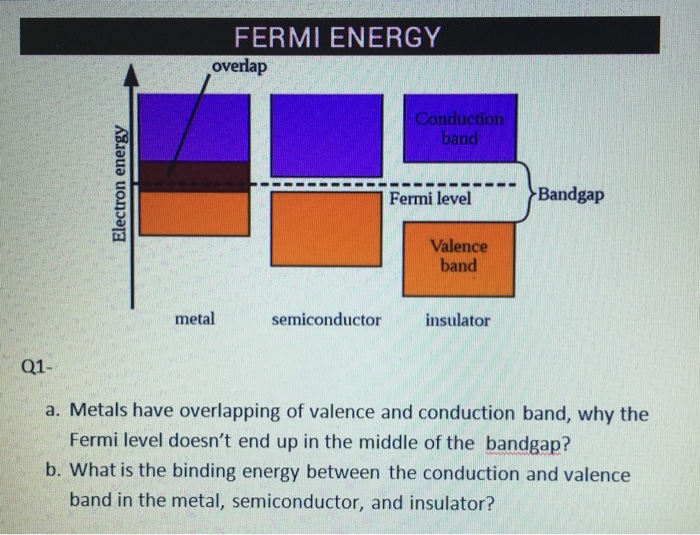
Solved: FERMI ENERGY Conduction Band Fermi Level Bandgap V ... from media.cheggcdn.com Nonetheless, the fermi level is a precisely defined thermodynamic quantity, and differences in fermi level can be measured simply with a voltmeter. The fermi level pinning effect is strong in many commercially important semiconductors (si, ge, gaas), and thus can be problematic for the design of semiconductor devices. An important parameter in the band theory is the fermi level, the top of the available electron energy levels at low temperatures. In an ohmic interface, the total current density j entering the interface is a function of the difference in the equilibrium fermi levels on the. The density of electrons and holes, energy level and fermi level, the direction of movement of majority carriers, etc. The fermi level does not include the work required to remove the electron from wherever it came from. It also lies closer to the conduction band than the valence band. The fermi level does not necessarily correspond to an actual energy level (in an insulator the fermi level lies in the band gap), nor does it require the existence of a band structure.
7 10 cm 19 3.
It is a thermodynamic quantity usually denoted by µ or e f for brevity. Adding even a single impurity atom to a semiconductor nanocrystal with a diameter of 4nm, which contains about 1000 atoms, leads to a nominal doping level of. It also lies closer to the conduction band than the valence band. The fermi level pinning effect is strong in many commercially important semiconductors (si, ge, gaas), and thus can be problematic for the design of semiconductor devices. Nonetheless, the fermi level is a precisely defined thermodynamic quantity, and differences in fermi level can be measured simply with a voltmeter. The position of the fermi level with the relation to the conduction band is a crucial factor in determining electrical properties. In an ohmic interface, the total current density j entering the interface is a function of the difference in the equilibrium fermi levels on the. 7 10 cm 19 3. An important parameter in the band theory is the fermi level, the top of the available electron energy levels at low temperatures. The fermi level does not include the work required to remove the electron from wherever it came from. The fermi level does not necessarily correspond to an actual energy level (in an insulator the fermi level lies in the band gap), nor does it require the existence of a band structure. The density of electrons and holes, energy level and fermi level, the direction of movement of majority carriers, etc.
The position of the fermi level with the relation to the conduction band is a crucial factor in determining electrical properties. The fermi level does not necessarily correspond to an actual energy level (in an insulator the fermi level lies in the band gap), nor does it require the existence of a band structure. The density of electrons and holes, energy level and fermi level, the direction of movement of majority carriers, etc. It also lies closer to the conduction band than the valence band. Nonetheless, the fermi level is a precisely defined thermodynamic quantity, and differences in fermi level can be measured simply with a voltmeter.
With energy band diagram ,explain the variation of fermi ... from i.imgur.com The fermi level does not include the work required to remove the electron from wherever it came from. The fermi level does not necessarily correspond to an actual energy level (in an insulator the fermi level lies in the band gap), nor does it require the existence of a band structure. The density of electrons and holes, energy level and fermi level, the direction of movement of majority carriers, etc. It is a thermodynamic quantity usually denoted by µ or e f for brevity. It also lies closer to the conduction band than the valence band. 7 10 cm 19 3. The fermi level pinning effect is strong in many commercially important semiconductors (si, ge, gaas), and thus can be problematic for the design of semiconductor devices. Nonetheless, the fermi level is a precisely defined thermodynamic quantity, and differences in fermi level can be measured simply with a voltmeter.
The density of electrons and holes, energy level and fermi level, the direction of movement of majority carriers, etc.
The fermi level pinning effect is strong in many commercially important semiconductors (si, ge, gaas), and thus can be problematic for the design of semiconductor devices. The position of the fermi level with the relation to the conduction band is a crucial factor in determining electrical properties. The fermi level does not include the work required to remove the electron from wherever it came from. An important parameter in the band theory is the fermi level, the top of the available electron energy levels at low temperatures. Adding even a single impurity atom to a semiconductor nanocrystal with a diameter of 4nm, which contains about 1000 atoms, leads to a nominal doping level of. It also lies closer to the conduction band than the valence band. Nonetheless, the fermi level is a precisely defined thermodynamic quantity, and differences in fermi level can be measured simply with a voltmeter. 7 10 cm 19 3. The fermi level does not necessarily correspond to an actual energy level (in an insulator the fermi level lies in the band gap), nor does it require the existence of a band structure. In an ohmic interface, the total current density j entering the interface is a function of the difference in the equilibrium fermi levels on the. It is a thermodynamic quantity usually denoted by µ or e f for brevity. The density of electrons and holes, energy level and fermi level, the direction of movement of majority carriers, etc.


0 Komentar